Project Radar Boards Schiphol Control: verschil tussen versies
(→ATMEGA 161L) |
|||
| Regel 65: | Regel 65: | ||
== ATMEGA 161L == | == ATMEGA 161L == | ||
| + | |||
| + | See also https://github.com/MakerSpaceLeiden/AirtrafficControlDisplaysSchiphol/blob/main/pins.h -- which has been tested against the actual board. | ||
{| class="wikitable" | {| class="wikitable" | ||
Versie van 11 jun 2021 om 22:01
We got a pile of Control Tower displays from Schiphol airport (or Eurocontrol, etc) used for tracking what is in the air.
They are basically small 2-3 CPU boards on a common RS 485 bus or on RS 232. One CPU is purely for programming. The other is the main board and handles the traffic on the bus (it may be ASTERIX format?) and the other handles the display. They are interconnected by a TTL serial on 9600 8N1. Each box also contains a high quality PSU.
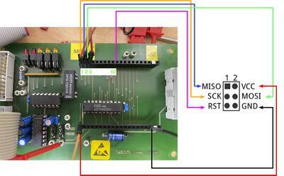
The programming chip is also 9600 8N1 and contains some debugging tooling. Photo below shows the testpoints used for programming.
But easiest may be to use normal ATMEL programmeing on MISO/MOSI - which are nicely broken out on the connector.
Rudimentary code: https://github.com/MakerSpaceLeiden/AirtrafficControlDisplaysSchiphol
Bestand:Schiphol-first-light.mov
Inhoud
Schiphol Airtraffic Control displays
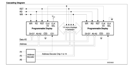
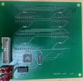
Seems to be the reference circuit from the display datasheet with an Atmel161:
With an SNx4HC138 3 line to 8 line decoder/demux used. De displays zijn niet op alle borden gelijk - maar wel uit de zelfde serie en aansturing.
Boards
Main connector
| 1 NC | 2 NC |
| 3 NC | 4 NC |
| 5 ? | 6 ? |
| 7 RST | 8 SCK |
| 9 MISO | 10 MOSI |
| 11 RX | 12 TX |
| 13 SS | 14 Vdd |
| 15 Vdd | 16 ? |
| 17 ? | GND |
| GND | GND |
Multiplexer
HC138 is een multiplexer (https://www.ti.com/lit/ds/symlink/sn74hc138.pdf?ts=1623312092250&ref_url=https%253A%252F%252Fwww.google.com%252F)
Pin 1,2,3 zijn de selects. 4,5 enables, G1 de active high
ABC worden alleen gebruikt - en schakelen het display
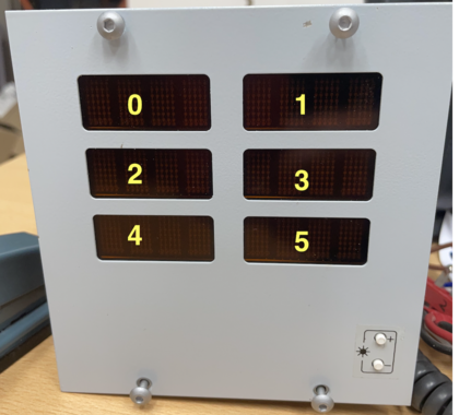
Multiplexer numbering
ATMEGA 161L
See also https://github.com/MakerSpaceLeiden/AirtrafficControlDisplaysSchiphol/blob/main/pins.h -- which has been tested against the actual board.
| 1 | MOSI - pin 9 connector |
| 2 | MISO - pin 10 connector |
| 3 | SCK - pin 8 connector |
| 4 | RST - pin 7 connector |
| 5 | RX - pin 11 connector |
| 6 | NC |
| 7 | TX - pin 12 connector |
| 8 | Brightness up to ground |
| 9 | Brightness down to ground |
| 10 | |
| 11 | |
| 12 | pin 10 display WR |
| 13 | pin 1 display RD |
| 14 | |
| 15 | |
| 16 | |
| 17 | |
| 18 | pin 9 display A0 |
| 19 | pin 8 display A1 |
| 20 | pin 7 display A2 |
| 21 | MCP 1 - 'A' select |
| 22 | MCP 2 - 'B' select |
| 23 | MCP 3 - 'C' select |
| 24 | pin 5 display CE1 |
| 25 | |
| 26 | pin 4 display RST |
| 27 | |
| 28 | |
| 29 | |
| 30 | pin 11 display D7 |
| 31 | pin 12 display D6 |
| 32 | pin 13 display D5 |
| 33 | pin 14 display D4 |
| 34 | pin 15 display D3 |
| 35 | pin 16 display D2 |
| 36 | pin 17 display D1 |
| 37 | pin 18 display D0 |
| 38 | VCC |
| 39 | |
| 40 | |
| 41 | |
| 42 | |
| 43 | |
| 44 | SS - pin 13 connector |
Display
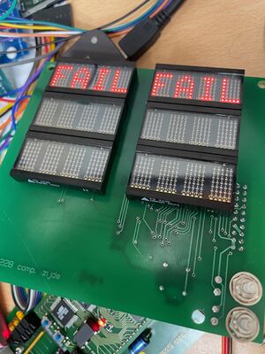
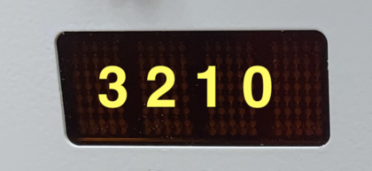
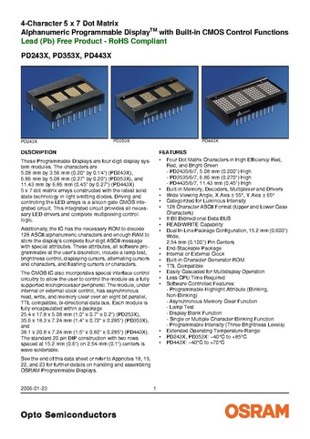
The various cards contains displays from the PD family.
Multiplexer numbering
Datasheet displays
The photo's are from the card with the 6 displays of type PD443.
Various people hack them
- https://www.flickr.com/photos/okini393939/5148872258
- https://github.com/TiNredmc/PD443X_Lib
- https://github.com/TiNredmc/PD443Xclock
Main Board
Connection on the main bord - top row near the yellow 'TOP1' label.
Wiring / pinout main CPU board
| TOP 1 | SCK of CPU display board |
| TOP 2 | MISO of CPU display board |
| TOP 3 | MOSI of CPU display board |
| TOP 10 | RST of CPU display board |
| TOP 13,14 | TX/RX of CPU display board |
| BOT far left/right | Power |
